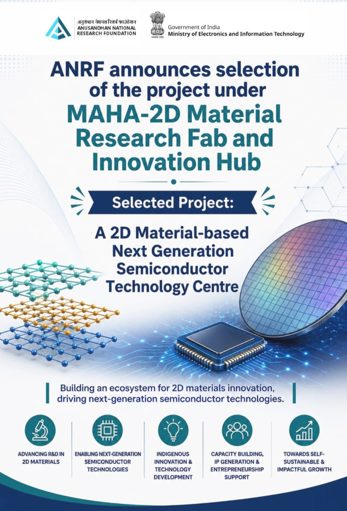
New Delhi, Aug 24 (INB) The Indian Institute of Science has been selected by the centre to set up the 2D Innovation Hub along with research and developed R&D Fab under the Mission for Advancement in High-impact Areas (MAHA) programme.
The Bengaluru based institute was selected by Anusandhan National Research Foundation (ANRF) and the Ministry of Electronics and Information Technology (MeitY) as part of their joint initiative to select entities eligible to advance research and development of 2D materials for semiconductors.
“Indian Institute of Science (IISc)-Bangalore-2D Innovation Hub: A 2D Material-based Next Generation Semiconductor Technology Centre. Led by Prof. Mayank Shrivastava, Department of Electronic Systems Engineering, IISc Bangalore, the Hub brings together 17 leading institutions as spoke partners from across India,” ANRF said in a social media post. 2D materials have potential to develop angstrom size semiconductor chips–which means chip equivalent 30th part of the smallest silicon chip of 2 nanometer available in the world.
The primary objective of the Hub is to establish a state-of-the-art 200-mm (8-inch) R&D Fab dedicated to 2D semiconductors. The facility will encompass an end-to-end framework—spanning raw materials and process engineering to Process Design Kits (PDKs), Multi-Project Wafer (MPW) runs, technology demonstrators, technology transfer, and startup incubation.
Over time, the Hub is envisioned to evolve into a broader national research and development platform for emerging semiconductor and quantum technologies, seamlessly linked with academia, industry, and top international research centres.
“This journey began with a white paper in 2018. Since then: years of discussions, reviews, revisions, stakeholder meetings, industry engagement, difficult phases, 100+ trips and eventually a national level evaluation. One lesson from this journey: ambitious ideas need perseverance as much as they need science,” Shrivastava said.
Emphasising a collaborative national footprint, the project brings together over 15 researchers from IISc, faculty across 18 SPOKE academic institutions, and more than 15 global and domestic industry leaders. The partner SPOKE institutes will focus on targeted, Hub-defined problem sets, operating on a model aligned closely with industry-funded academic R&D.
𝗕𝗮𝗻𝗮𝗿𝗮𝘀 𝗛𝗶𝗻𝗱𝘂 𝗨𝗻𝗶𝘃𝗲𝗿𝘀𝗶𝘁𝘆 , 𝗜𝗜𝗧 (𝗜𝗦𝗠) 𝗗𝗵𝗮𝗻𝗯𝗮𝗱 , 𝗜𝗜𝗧 𝗞𝗮𝗻𝗽𝘂𝗿 , 𝗜𝗜𝗧 𝗣𝗮𝘁𝗻𝗮 , 𝗜𝗜𝗧 𝗛𝘆𝗱𝗲𝗿𝗮𝗯𝗮𝗱 , 𝗡𝗜𝗧 𝗦𝗿𝗶𝗻𝗮𝗴𝗮𝗿 , 𝗜𝗜𝗜𝗧 𝗔𝗹𝗹𝗮𝗵𝗮𝗯𝗮𝗱 , 𝗜𝗜𝗧 𝗗𝗲𝗹𝗵𝗶 , 𝗜𝗜𝗧 𝗠𝗮𝗱𝗿𝗮𝘀 , 𝗜𝗜𝗦𝗘𝗥 𝗕𝗵𝗼𝗽𝗮𝗹 , 𝗜𝗜𝗦𝗘𝗥 𝗧𝗵𝗶𝗿𝘂𝘃𝗮𝗻𝗮𝗻𝘁𝗵𝗮𝗽𝘂𝗿𝗮𝗺 , 𝗕𝗜𝗧𝗦 𝗣𝗶𝗹𝗮𝗻𝗶, 𝗛𝘆𝗱𝗲𝗿𝗮𝗯𝗮𝗱 𝗖𝗮𝗺𝗽𝘂𝘀 , 𝗣𝗹𝗮𝗸𝘀𝗵𝗮 𝗨𝗻𝗶𝘃𝗲𝗿𝘀𝗶𝘁𝘆 , 𝗜𝗜𝗜𝗧𝗗𝗠 𝗞𝗮𝗻𝗰𝗵𝗲𝗲𝗽𝘂𝗿𝗮𝗺 , 𝗜𝗜𝗧 𝗞𝗵𝗮𝗿𝗮𝗴𝗽𝘂𝗿 , 𝗖-𝗠𝗘𝗧 𝗣𝘂𝗻𝗲 and 𝗜𝗜𝗘𝗦𝗧 𝗦𝗵𝗶𝗯𝗽𝘂𝗿 will work as spoke partner of IISc under this hub and spoke model finalised by the centre.
The Hub, which is IISc in this case, will remain open to expanding its network, inviting interest from researchers across the country and globally to ensure the platform eventually benefits the broader semiconductor and quantum research communities.
“We are also open to growing this network and welcome interest from other 2D researchers. Eventually, the Hub should benefit every 2D semiconductor/quantum researcher in India and the world,” Shrivastava said.